The HackerFab at IIT Bombay demonstrates that semiconductor fabrication tools can be built and operated by students at significantly lower costs than commercial equipment, making hands-on semiconductor education accessible to students who would otherwise never touch a silicon wafer. The facility uses a DLP-based maskless lithography machine (10um resolution), a quartz tube furnace reaching 1,200°C for oxidation and annealing, and a DC plasma sputter for metal deposition, all constructed from repurposed components and secondhand parts. This approach enables students to gain practical fabrication experience, develop intuition for process optimization, and potentially tap out transistors by graduation, addressing the critical gap in India's semiconductor education ecosystem where most electrical engineers never get hands-on experience with semiconductor fabrication.
Install our extension to search inside any video instantly.
A Fab Like This Doesn't Exist Anywhere Else in India Right Now
Added:Related Videos

BMW Built A Radial Engine So Good It Made The Spitfire Obsolete Overnight
MachineTitans999
123 views•2026-06-18

The Bizarre Design Flaw That Ruined The Convair 990
Jet-Deck
631 views•2026-06-19
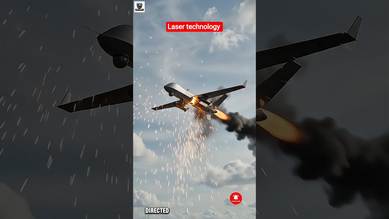
US Navy's Helios laser tech
Striketech0310
6K views•2026-06-18

Grandma's Best fan placement to move air through the house
DalesGrandpasSecrets
613 views•2026-06-19

Semi automatic quick coupler and diverter valve tool for mini excavators
rgtoutdoors7130
287 views•2026-06-21

Why Does Concrete Need a ‘Curing’ Phase?
historyofsimplethings
207 views•2026-06-18

3 Minutes Later! Huge Russian Motorcycles and Quad Bikes Troops Enter Pokrovsk - Scott Ritter
ScottRitterUpdates
266 views•2026-06-20

Ogbunike Bypass linking 2nd Niger Bridge ️ Road Expansion in Awka, Anambra
ArlinTv
335 views•2026-06-19